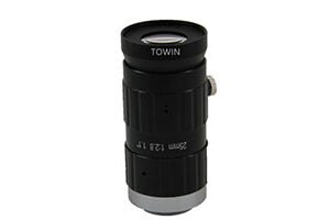
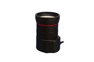
In modern electronics manufacturing, precision is non-negotiable. A single misaligned component or solder joint can lead to product failures, costly recalls, and reputational damage. Enter the Electronics Assembly Verification Lens—a specialized Industrial Lens designed to revolutionize quality control in assembly lines.
Why the Electronics Assembly Verification Lens Matters in Industrial Settings
The Electronics Assembly Verification Lens is not just another camera or magnifier; it’s a high-precision Industrial Lens engineered to detect microscopic defects that human eyes or traditional tools might miss. From solder paste inspection to component placement verification, this lens provides real-time feedback, enabling manufacturers to catch errors before they escalate.
Key Applications:
- Solder Joint Analysis: Identifies voids, cracks, or uneven solder distribution.
- Component Alignment: Verifies the exact positioning of microchips, resistors, and capacitors.
- Surface Defect Detection: Spots scratches, contaminants, or irregularities on PCBs (Printed Circuit Boards).
- Traceability: Captures detailed images for audit trails and compliance reporting.
By integrating the Electronics Assembly Verification Lens into automated systems, manufacturers achieve 99.9% accuracy rates, reducing waste and boosting productivity.
How the Electronics Assembly Verification Lens Works
This Industrial Lens operates on a blend of optical coherence tomography (OCT) and machine learning algorithms. Here’s a breakdown of its workflow:
- Image Capture: The lens scans the assembly surface at high resolution, capturing millions of data points per second.
- Defect Detection: AI-powered software analyzes images, comparing them against predefined quality benchmarks.
- Real-Time Feedback: Alerts operators or robots to correct anomalies immediately, preventing defective units from progressing downstream.
Unlike manual inspections, which are prone to human error, the Electronics Assembly Verification Lens delivers consistent, objective results 24/7.
Advantages of Using an Industrial Lens for Electronics Assembly
- Unmatched Precision: Detect defects as small as 10 microns, far beyond human capability.
- Speed: Process hundreds of assemblies per hour without compromising accuracy.
- Cost Savings: Reduce rework and scrap rates by up to 70%, saving thousands annually.
- Scalability: Seamlessly integrate with existing SMT (Surface Mount Technology) lines or robotic systems.
- Compliance: Meet ISO 9001 and IPC-A-610 standards effortlessly with documented inspection data.
Common Challenges & Solutions
While the Electronics Assembly Verification Lens is transformative, it’s not without hurdles. Here’s how to overcome them:
Challenge 1: High Initial Cost
Solution: Amortize costs over time through reduced waste and higher throughput. Many suppliers offer leasing options.
Challenge 2: Integration Complexity
Solution: Partner with vendors like Keyence or Cognex, who provide turnkey solutions and training.
Challenge 3: Lighting Variability
Solution: Use coaxial or ring lighting to eliminate shadows and glare, ensuring consistent image quality.
FAQs
What makes the Electronics Assembly Verification Lens different from standard magnifiers?
Standard magnifiers rely on subjective human interpretation, while this Industrial Lens combines high-resolution optics with AI for objective, data-driven analysis.
Can it inspect both rigid and flexible PCBs?
Yes! The lens adapts to various substrates, including rigid FR4 boards and flexible polyimide circuits.
How often does the lens need calibration?
Most systems require calibration every 6–12 months, depending on usage. Automated calibration tools simplify this process.
Is it compatible with Industry 4.0 protocols?
Absolutely. The Electronics Assembly Verification Lens supports IoT integration, enabling remote monitoring and predictive maintenance.
What industries benefit most from this technology?
Automotive, aerospace, medical devices, and consumer electronics manufacturers see the highest ROI due to their strict quality requirements.
Conclusion
The Electronics Assembly Verification Lens is more than a tool—it’s a game-changer for Industrial Lens applications. By merging cutting-edge optics with AI, it empowers manufacturers to achieve zero-defect production while slashing costs.